Ca Antivirus Cookies Help
Download free CA AntiVirus Plus Anti-Spyware 2010: Clean your computer after you download CA AntiVirus. Detect and eliminate potential security threats with the.
CA Technologies offers IT management software and solutions for all of your business needs.
Tracking Cookie removal - Symantec Security Response provides comprehensive internet protection expertise to guard against complex threats, information about latest.
Contact PCPlanet for CA Antivirus Support Help The world of computing technology is ever dynamic and changing. PCPlanet helps consumers globally get the best.
AVG AntiVirus Protection FREE; AVG TuneUp Performance FREE; AVG Ultimate; Google Analytics makes use of cookies to help AVG analyze how users use our.
Protecting over 30 Million users
Limited-time offer: Save 25 10 off
Every day, hackers release thousands of viruses and other malware.
And Webroot protects millions of people against them.
Phishing Attacks Fake Websites
Lightning fast scans in minutes
Microsoft Windows XP 32- and 64-bit SP2, SP3
Windows Vista 32-bit all Editions, Windows Vista SP1, SP2 32- and 64-bit all Editions
Windows 7 32- and 64-bit all Editions, Windows 7 SP1 32- and 64-bit all Editions
Intel Pentium /Celeron family, or AMD K6/Athlon /Duron family, or other compatible processor
Microsoft Internet Explorer 7.0 and higher, Mozilla Firefox 3.6 and higher 32-bit only, Google Chrome 10.0 or higher
Mac OS X v. 10.8 Mountain Lion
Download the PassMark Performance Benchmark
Webroot uses 143x less disk space than the next closest competitor. This chart compares the total size of files added during the installation of Antivirus products. Products with lower installation sizes are considered better performing products in this Category.
Webroot uses 11x less computer memory than the closest competitor during system idle. This chart compares the average amount of RAM in use by an Antivirus product during a perioid of system idle. This average is taken from a sample of ten memory snapshots taken at roughly 60 seconds apart after reboot. Products with lower idle RAM usage are considered better performing products in this category.
We re also the fastest in scheduled scans at 1 minute 12 seconds – 16x faster than the competitor average. This chart compares the average time taken to run a system scan at a specified time. Products with lower scan times are considered better performing in this category.
Webroot security is up and running in 5 seconds – 38x faster than the competitor average. This chart compares the minimum installation time it takes for Antivirus products to be fully functional and ready for use by the end user. Products with lower installation times are considered better performing products in this category.
Webroot SecureAnywhere AntiVirus is tiny beyond belief, yet it achieved perfect scores across the board in my malware-blocking tests. It also did a very good job cleaning up malware-infected systems.
Webroot honors a 70-day money back guarantee for all consumer products.
Choose Your Level of Protection
Looking for business solutions.
Advanced threat protection for PC Mac
Always-on security for your data and identity
Real-Time Anti-Phishing blocks harmful websites
Firewall and network connection monitor
Lightning fast scans without interruptions
Secures your smartphones and tablets
Protects account logins and passwords
Eliminates traces of online activity
25GB of secure online storage, accessible from all your devices
Protects your account logins and passwords
Makes deleted files unrecoverable
Webroot is internationally recognized for providing world-class internet security software and solutions.
Offered in the 50 U.S. between PM MT on October 15, 2015 and PM MT on March 31, 2016 Offer Period. During the Offer Period, you will receive 25 off the purchase price excluding applicable taxes when you purchase a 1 year / 3 device subscription to Webroot SecureAnywhere AntiVirus, 25 off the purchase price excluding applicable taxes when you purchase a 1 year / 3 device subscription to Webroot SecureAnywhere Internet Security Plus, or 25 off the purchase price excluding applicable taxes when you purchase a 1 year / 5 device subscription to Webroot SecureAnywhere Complete. Offer applies only to subscriptions purchased from www.webroot.com or by phone at 866-612-4268, and is available only while supplies last. Not valid on previously purchased or out-of-stock merchandise. May not be combined with any other offer, coupon or discount. Webroot reserves the right to modify, cancel or terminate this offer at any time without notice. Void where taxed, restricted or prohibited, and to employees of Webroot and participating online affiliates.
Offered in the United Kingdom between PM MT on October 15, 2015 and PM MT on March 31, 2016 Offer Period. During the Offer Period, you will receive 25 off the purchase price excluding applicable taxes when you purchase a 1 year / 3 device subscription to Webroot SecureAnywhere AntiVirus, 25 off the purchase price excluding applicable taxes when you purchase a 1 year / 3 device subscription to Webroot SecureAnywhere Internet Security Plus, or 25 off the purchase price excluding applicable taxes when you purchase a 1 year / 5 device subscription to Webroot SecureAnywhere Complete. Offer applies only to subscriptions purchased from www.webroot.com or by phone at 44 0 870 141 7070, and is available only while supplies last. Not valid on previously purchased or out-of-stock merchandise. May not be combined with any other offer, coupon or discount. Webroot reserves the right to modify, cancel or terminate this offer at any time without notice. Void where taxed, restricted or prohibited, and to employees of Webroot and participating online affiliates.
Offered in Australia between PM MT on October 15, 2015 and PM MT on March 31, 2016 Offer Period. During the Offer Period, you will receive 25 off the purchase price excluding applicable taxes when you purchase a 1 year / 3 device subscription to Webroot SecureAnywhere AntiVirus, 25 off the purchase price excluding applicable taxes when you purchase a 1 year / 3 device subscription to Webroot SecureAnywhere Internet Security Plus, or 25 off the purchase price excluding applicable taxes when you purchase a 1 year / 5 device subscription to Webroot SecureAnywhere Complete. Offer applies only to subscriptions purchased from www.webroot.com or by phone at 1-800-014-772, and is available only while supplies last. Not valid on previously purchased or out-of-stock merchandise. May not be combined with any other offer, coupon or discount. Webroot reserves the right to modify, cancel or terminate this offer at any time without notice. Void where taxed, restricted or prohibited, and to employees of Webroot and participating online affiliates.
CA Support: How can we help. Helping you meet your business needs and get the most from your CA solution.


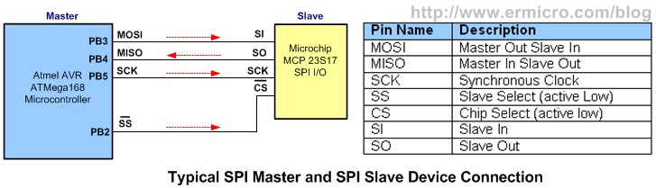
Serial Port Spi
Blog Entry Using Serial Peripheral Interface SPI Master and Slave with Atmel AVR Microcontroller June 25, 2009 by rwb, under Microcontroller. Sometimes we need to.
Sometimes we need to extend or add more I/O ports to our microcontroller based project. Because usually we only have a limited I/O port left than the logical choice is to use the serial data transfer method; which usually only requires from one up to four ports for doing the data transfer. Currently there are few types of modern embedded system serial data transfer interface widely supported by most of the chip s manufactures such as I2C read as I square C, SPI Serial Peripheral Interface, 1-Wire One Wire, Controller Area Network CAN, USB Universal Serial Bus and the RS-232 families RS-423, RS-422 and RS-485. The last three interface types is used for long connection between the microcontroller and the devices, up to 1200 meters for the RS-485 specification, while the first three is used for short range connection.
Among these serial data transfer interface types, SPI is considered the fastest synchronous with full duplex serial data transfer interface and can be clocked up to 10 MHz; that is why it is widely used as the interface method to the high speed demand peripheral such as the Microchip Ethernet controller ENC28J60, Multi Media Card MMC Flash Memory, Microchip SPI I/O MCP23S17, Microchip 128K SPI EEPROM 25AA128, ADC, sensors, etc.
In this tutorial we will learn how to utilize the Atmel AVR ATMega168 SPI peripheral to expand the ATMega168 I/O ports and to communicate between two microcontrollers with the SPI peripheral where one microcontroller is configured as a master and other as a slave. The principal we learn here could be applied to other types of microcontroller families.
Serial Peripheral Interface SPI
The standard Serial Peripheral Interface uses a minimum of three line ports for communicating with a single SPI device SPI slave, with the chip select pin CS is being always connected to the ground enable. If more the one SPI devices is connected to the same bus, then we need four ports and use the fourth port SS pin on the ATMega168 microcontroller to select the target SPI device before starting to communicate with it.
If more then three SPI slave devices, then it is better to use from three to eight channels decoder chip such as 74HC138 families. Since the SPI protocol uses full duplex synchronous serial data transfer method, it could transfer the data and at the same time receiving the slave data using its internal shift register.
From the SPI master and slave interconnection diagram above you could see that the SPI peripheral use the shift register to transfer and receive the data, for example the master want to transfer 0b10001101 0x8E to the slave and at the same time the slave device also want to transfer the 0b00110010 0 32 data to the master. By activating the CS chip select pin on the slave device, now the slave is ready to receive the data. On the first clock cycle both master and slave shift register will shift their registers content one bit to the left; the SPI slave will receive the first bit from the master on its LSB register while at he same time the SPI master will receive its first data from slave on its LSB register.
Continuously using the same principal for each bit, the complete data transfer between master and slave will be done in 8 clock cycle. By using the highest possible clock allowed such as the Microchip MCP23S17 SPI slave I/O device 10 MHz than the complete data transfer between the microcontroller and this SPI I/O port could be achieve in 0.8 us. As you understand how the SPI principal works, now its time to implement it with the Atmel AVR ATMega168 microcontroller.
The following is the list of hardware and software used in this project:
74HC595, 8-bit shift registers with output latch
Microchip MCP23S17 16-bit SPI I/O Expander
AVRJazz Mega168 board from ermicro which base on the AVR ATmega168 microcontroller board schema.
WinAVR for the GNU s C compiler
Atmel AVR Studio 4 for the coding and debugging environment
STK500 programmer from AVR Studio 4, using the AVRJazz Mega168 board STK500 v2.0 bootloader facility.
Expanding Output Port with 74HC595 8-bit Shift Registers
Because the basic operation of SPI peripheral is a shift register, then we could simply use the 8-bit shift register with output latch to expand the output port. The 16 pins 74HC595 families could be use to serve this purpose.
The 74HC595 device has 8-bit serial-in, parallel-out shift register that feeds directly to the 8-bit D-type storage register. The 8-bit serial-in shift register has its own input clock pin named SCK, while the D-Latch 8-bit registers use pin named RCK for transferring latching the 8-bit shift registers output to D-Latch output registers.
In normal operation according to the truth table above the 74HC595 shift registers clear pin SCLR should be put on logical high and the 8-bit D-Latch buffer output enable pin G should be put on logical low. By feeding the serial input pin SER with AVR ATMega168 master out slave in pin MOSI and connecting the master synchronous clock SCK to the 74HC595 shift registers clock SCK, we could simply use the 74HC595 as the SPI slave device. Optionally we could connect the 74HC595 Q H output pin shift registers MSB bit to the master in slave out pin MISO ; this optional connection will simply returns the previous value of the shift registers to the SPI master register.
Now let s take a look to the C code for sending simple chaser LED display to the 74HC595 output:
// Description : SPI I/O Using 74HC595 8-bit shift registers
// Target : AVRJazz Mega168 Board
// Compiler : AVR-GCC 4.3.0; avr-libc 1.6.2 WinAVR 20080610
// IDE : Atmel AVR Studio 4.14
// Programmer : AVRJazz Mega168 STK500 v2.0 Bootloader
// : AVR Visual Studio 4.14, STK500 programmer
unsigned char SPI_WriteRead unsigned char dataout
// Wait for transmission complete
// Latch the Output using rising pulse to the RCK Pin
_delay_us 1 ; // Hold pulse for 1 micro second
// Return Serial In Value MISO
// Initial the AVR ATMega168 SPI Peripheral
// Set MOSI and SCK as output, others as input
// Enable SPI, Master, set clock rate fck/2 maximum
AVR Serial Peripheral Interface
The principal operation of the SPI is simple but rather then to create our own bit-bang algorithm to send the data, the build in SPI peripheral inside the Atmel AVR ATMega168 microcontroller make the SPI programming become easier as we just passing our data to the SPI data register SPDR and let the AVR ATMega168 SPI peripheral do the job to send and read the data from the SPI slave device. To initialize the SPI peripheral inside the ATMega168 microcontroller we need to enable this device for SPI master and set the master clock frequency using the SPI control register SPCR and SPI status register SPST, for more information please refer to the AVR ATMega168 datasheet.
The first thing before we use the SPI peripheral is to set the SPI port for SPI master operation; MOSI PB3 and SCK PB5 as output port and MISO PB4 is the input port, while the SS can be any port for SPI master operation but on this tutorial we will use the PB2 to select the SPI slave device. The following C code is used to set these SPI ports.
After initializing the ports now we have to enable the SPI by setting the SPE SPI enable bit to logical 1 and selecting the SPI master operation by setting the MSTR bit to logical 1 in the SPCR register. For all other bits we just use its default value logical 0 ; such as the data order DORD bit for first transferring MSB, using the rising clock for the master clock on clock polarity CPOL bit and sampled the data on leading edge clock phase CPHA bit.
Because the 74HC595 shift register can receive up to 30 Mhz clock rate, then I use the fastest clock that can be generated by the ATMega168 microcontroller SPI peripheral which is fsc/2 the AVRJazz Mega168 board using 11.059200 MHz ; therefore the maximum clock generated by the SPI master will be 5.5296 MHz. This frequency can be achieved by setting the SPR1 0 and SPR0 0 in the SPCR register and SPI2X 1 in the SPSR register.
// Enable SPI, Master, set clock rate fck/2 maximum
Sending and reading the data is using the SPI data register SPDT and when the SPI Master-Slave data transfer is completed than SPIF SPI interrupt flag in the SPSR register will be set to logical 1 ; therefore by examining this bit status we could ensure that the transmission between SPI master and slave is completed.
After reading the data from the SPDT register; we have to send the latch clock to the 74HC595 D-Latch register RCK pin to latch the 8-bit shift registers data to its output.
Microchip MCP23S17 SPI I/O Expander
For more advance input and output capability SPI device you could use the Microchip MCP23S17 SPI I/O Expander chip, which provide additional 16-bit I/O for your microcontroller s based project.
With the addressable pins configuration feature A2,A1 and A0, practically you could attach up to 8 of MCP23S17 SPI I/O expander devices which gives you 128 I/O ports using just four of your AVR ATMega168 microcontroller s ports MOSI, MISO, SCK and SS.
All the MCP23S17 16-bit general purpose I/O GPIO ports can be configured both as input or output by setting the MCP23S17 IODIRA and IODIRB I/O direction register. Each of the MCP23S17 general I/O pins could be configured to generate interrupt when the ports pin changes its state for more information please refers to Microchip MCP23S17 datasheet.
For the purpose of this tutorial we will use the Microchip MCP23S17 just as the ordinary input and output expander for the AVR ATMega168 microcontroller.
The MCP23S17 is configured to use address 0 00 address pins A0,A1 and A2 are connected to the ground and the push button switch connected to GPB0 port will be use as the toggle button to start and stop the chaser LED display attached to the GPA0 to GPA7 ports. The following is the C code to achieve these tasks.
// Description : SPI I/O Using Microchip MCP23S17 16-Bit I/O Expander
define SPI_SLAVE_ADDR 0x00 // A2 0,A1 0,A0 0
// MCP23S17 Registers Definition for BANK 0 default
// Define MCP23S17 Slave Emulation Mode:
// Only works on real Microchip MCP23S17 SPI I/O
// 1 - ATMega168 SPI Slave MCP23S17 Emulation :
// Both works on real MCP23S17 and ATMega168 Slave Mode
// ATMega168 Crystal Frequency: 11059200 Hz
void SPI_Write unsigned char addr,unsigned char data
// Start MCP23S17 OpCode transmission
SPDR SPI_SLAVE_ID SPI_SLAVE_ADDR
// Start MCP23S17 Register Address transmission
unsigned char SPI_Read unsigned char addr
// Start MCP23S17 Address transmission
// Send Dummy transmission for reading the data
unsigned char cnt,togbutton,inp;
// Initial ATMega168 ADC Peripheral for User s Trimpot Input on PC0
// Disable digital input on ADC0 PC0
ADMUX 0x00; // Select Channel 0 PC0
// Set MOSI PB3, SCK PB5 and PB2 SS as output, others as input
// Enable SPI, Master, set clock rate fck/64
// Enable SPI, Master, set clock rate fck/2
// Initial the MCP23S17 SPI I/O Expander
SPI_Write IOCONA,0x28 ; // I/O Control Register: BANK 0, SEQOP 1, HAEN 1 Enable Addressing
SPI_Write IODIRA,0x00 ; // GPIOA As Output
SPI_Write IODIRB,0xFF ; // GPIOB As Input
SPI_Write GPPUB,0xFF ; // Enable Pull-up Resistor on GPIOB
SPI_Write GPIOA,0x00 ; // Reset Output on GPIOA
inp SPI_Read GPIOB ; // Read from GPIOB
if inp 0xFE // Button is pressed
inp SPI_Read GPIOB ; // Read from GPIOB, for simple debounce
SPI_Write GPIOA,0x00 ; // Write to MCP23S17 GPIOA
// Start conversion by setting ADSC on ADCSRA Register
// wait until convertion complete ADSC 0 - Complete
SPI_Write GPIOA,pattern cnt ; // Write to MCP23S17 GPIOA
PORTD pattern cnt ; // Write to PORTD
Unlike the 74HC595 8-bit shift register above, writing and reading to and from the MCP23S17 SPI slave must be done in three SPI master writing operation cycles. First the SPI master has to send the MCP23S17 SPI slave ID with its physical address set by A2, A1 and A0 pins and the read or write instruction to the MCP23S17. Secondly the SPI master has to tell MCP23S17 which one of the MCP23S17 control registers address we want to use, and the last one we send or read the actual data.
From the MCP23S17 SPI addressing diagram above you could see that at least we need to perform three SPI master writing to send or read the data to or from the MCP23S17 SPI slave I/O expander. Using the same principal we ve learned from the 74HC595 to send the data we simply supply the correct data to the ATMega168 microcontroller SPDR register while keep the SS PB2 pin low to enable the MCP23S17 SPI slave device. After all data has been sent or read then we raise logical 1 the SS PB2 pin to deactivate the SPI slave device.
The SPI_Write and the SPI_Read function are used to do the write and read to and from the MCP23S17 SPI slave. As you ve seen from the SPI_Read function code above because the SPI slave could not initiate its own data transfer therefore the SPI master has to start the data transfer by sending the dummy data 0 00 to the SPI slave in order to read the SPI slave data.
The MCP23S17 SPI I/O expander has two general I/O ports named GPIOA and GPIOB. The default power-up condition of MCP23S17 is all I/O ports configured as an input port. By changing each of the I/O direction registers IODIRA and IODIRB we could change this port behavior; this pretty much the same as we set the data direction register on the ATMega168 microcontroller I/O ports. The following code shows how to initialize the MCP23S17 SPI I/O expander.
SPI_Write IOCONA,0x28 ; // I/O Control Register: BANK 0, SEQOP 1, HAEN 1 Enable Addressing
By assigning the IODIRA with 0 00 and IODIRB with 0xFF, we tell MCP23S17 to assign its GPIOA ports as output and GPIOB as input. Remember this setup is different compare to the ATMega168 microcontroller data direction register, which use 0xFF for output and 0 00 for input. To make sure all the GPIOB input ports are on known state all ports high, we activate the MCP23S17 pull-up resistors by assigning 0xFF to the GPPUB register.
To enable the MCP23S17 addressing mode, we have to enable logical 1 the HAEN bit on the IOCONA register. The IOCONA and IOCONB registers actually shared the same bit; therefore you could change either the IOCONA or IOCONB.
Assigning 0 28 to the IOCON register means we used the BANK 0 addressing mode, disable the sequential address increment and we enable the address bit control on A2, A1 and A0 pins of MCP23S17 current implementation A2 0, A1 0, and A0 0.
After configure the MCP23S17 registers, we entering the infinite loop which simple read the MCP23S17 GPIOB input port and if the switch is pressed then start sending the LED display patterns to the MCP23S17 GPIOA output port and to the ATMega168 PORTD which is also configured as the output port.
The LED display delay is controlled by the user s trimport on the AVRJazz Mega168 board which connected to the ADC channel 0 PC0, for further information about using the ATMega168 microcontroller ADC peripheral please refer to my previous posted blog Analog to Digital Converter AVR C Programming.
AVR ATMega168 microcontroller as the SPI Slave Device
In this last AVR SPI tutorial we will transform a second AVR ATMega168 to the SPI slave I/O device; in order not to change the SPI master demo program shown on the MCP23S17 section above, I decided to emulate some functions of the Microchip MCP23S17 SPI I/O expander using the Atmel AVR ATMega168 microcontroller and at the same time it will give us a good example of how to program the AVR ATMega168 microcontroller as the SPI slave device.
The SPI slave device practically is a passive device which means that the SPI device could not initiate the data transfer to the SPI Master. Its rely only on the SPI Master to first transfer its data then at the same time the SPI slave could transfer its own data to the SPI master. The C code bellows show how the Atmel AVR ATMega168 microcontroller being transformed to the Microchip MCP23S17 SPI I/O expander:
// Description : SPI I/O Using ATMega168 as the SPI Slave device
// Partial Emulation of MCP23S17 SPI I/O Expander
// PORTD - GPIOA, PORTB.PB0 - GPIOB.GPB0
// MCP23S17 Emulation Read Write OpCode
unsigned char datain,dataout,slavereg;
// MCP23S17 Registers Emulation Variables
// Initial the AVR ATMega168 SPI Slave Peripheral
// Set MISO PB4 as output, others as input
state 0; // State: 0-ID and Address, 1-Register, 2-Data
// Reset All the MCP23S17 Slave Emulation Registers
datain SPI_WriteRead dataout ;
// Check for MCP23S17 Slave Emulation OpCode
// For MCP23S17 implemented register, change the state
if datain IODIRA datain IODIRB datain IOCONA datain GPPUA
datain GPPUB datain GPIOA datain GPIOB
// For Read Condition then prepare for returning value on the next master cycle
// Complement Data, ATMega168 DDR use 1 for Output Data Direction
iodirb datain 0x01; // Just put it on variable
// Only for input PB0, ignore output and other ports
iocona datain; // Just put it on variable
gppua datain; // Just put it on variable
gppub datain; // Just put it on variable
PORTD datain; // Passing data to the real port
gpiob datain; // Passing data to the emulation register
The ATMega168 microcontroller SPI slave initiation can be done by simply enabling the MISO port PB4 as the output port and enabling the SPI peripheral bit SPE logical 1 in the SPCR register. By polling the SPDR register using the SPI_WriteRead function we could examine the data send by the SPI Master using the state condition algorithm to emulate the Microchip MCP23S17 SPI I/O expander partial functionality as shown inside the infinite loop code.
The first state cycle checks if the SPI master is sending the MCP23S17 ID 0100 and the address currently implemented as 000 and examines if this is READ 1 or WRITE 0 operation code.
The second state cycle check for implemented MCP23S17 control registers IODIRA, IODIRB,IOCONA,GPPUA,GPPUB,GPIOA, and GPIOB and at the same time prepares the data to be sent to the SPI Master on the next SPI master cycle if this is the READ operation
The third state cycle final state send the SPI slave data to the SPI master, executes the WRITE operation using the last data sent by the SPI master to the MCP23S17 emulated registers and resets the state cycle variables for the next new SPI master command.
If you notice in the SPI master code above MCP23S17 section, I include the define MCP23S17_EMULATION 1 compiler directive; which give slightly different code when it turn off define MCP23S17_EMULATION 0.
When you turn off this compiler directive the SPI master clock setting will use the fastest possible clock fsck/2 5.5296 MHz, but this clock rate will not work on the ATMega168 SPI slave, it only work on real Microchip MCP23S17 SPI I/O expander; therefore for the ATMega168 SPI slave we use the fck/64 172.800 KHz with 11.059200 MHz crystal clock on the AVRJazz Mega168 board.
Now you could enjoy the following video showing all the experiments we ve done in this tutorial:
Currently the Serial Peripheral Interface SPI is lack of the standard specification, its also called de facto standard, rather than one standard protocol specification agreed by the international committee. This lack of the standardization lead to the wide SPI protocol option implemented by various manufactures; for example as shown on the SPI data transfer to the 74HC595 8-bit shift register tutorial above, we use different chip select logical signal to latch the 74HC595 D-Latch register compared to the real SPI slave I/O device such as Microchip MCP23S17.
Nevertheless the SPI is out there; it s still considered as one of the best and fastest embedded systems serial data transfers available today and it s supported by most of the IC integrated circuit leading manufactures.
You must be logged in to post a comment.
AVRJazz Mega168/328 Learning and Development Board
November 11, 2008 by admin, under Development Board News.
The AVRJazz Mega168 board from ermicro is designed to be used both as the AVR microcontroller learning and development board. The AVR Jazz Mega168 board is stand alone microcontroller module equipped with the latest Atmel high performance low power technology AVR ATMega168 or ATMega328 microcontroller that can be used for wide range of applications including embedded controller, remote data logger, robotics and much more.
The AVRJazz Mega168 board features
High performance low power Atmel ATMega168 microcontroller with 16 Kbytes Self-Programmable Flash 2 Kbytes used for bootloader program, 512 Kbytes EEPROM and 1Kbytes Internal SRAM. Peripherals include: two 8 bit and one 16 Bit Timers/Counter, six PWM channels, six-channels 10 bit ADC, Analog Comparator, USART, Master/Slave SPI and I2C
Eight 3mm blue LED attached to the Port D through 74HCT240 buffer
One user potentiometer for analog input
Adjustable ADC Voltage reference
Buzzer for playing sound connected to one of the AVR 16bit PWM channel
High speed instruction throughput using 11 Mhz Crystal
RS232 Level converter for communicating with other equipment such as PC
LM35DZ Precision Centigrade Temperature Sensor for measuring temperature
Microchip 16 Kbytes I2C EEPROM using 24AA128 for data storage
Fully supported by Atmel AVR Studio 4 and AVR-GCC
Compatible with Arduino Integrated Development Environment which give you more flexible programming environment Windows or Linux and lots of program examples from the Arduino forum
STK500 v2.0 compatible preprogrammed boot loader, no external hardware is required to re programmed the AVRJazz Mega168 board
ISP Port to re programmed the AVRJazz Mega168 board with Atmel AVR ISP programmer such as Atmel AVRISP mkII
The AVRJazz Mega168 board microcontroller socket is pin compatible with Atmel 8-bit 28 pins microcontrollers such as ATMega44 4K, ATMega8 8K, ATMega88 8K, ATMega168 16K and ATMega328 32K.
Example project using AVRJazz Mega168 board could be found on ermicroblog
The AVRJazz Mega168 board demo program source code is include in the CDROM; this program demonstrate the capability of the AVRJazz Mega168 board such as accessing the I2C 24AA128 EEPROM, reading the LM35DZ centigrade temperature sensor, using the RS232 port, using the user switch, using the user analog input trimport and running the eight 3mm blue LED.
Running the AVRJazz Mega168 demonstration program
The AVRJazz Mega168 Board comes preprogrammed with a demonstration program. To use this program, connect the AVRJazz to the battery power that come with the board. The demo program will display the chasing light on the eight blue LED mode 0. Rotate the user trimport, labeled R12, and the chasing led speed will change in different rate. Press the user switch, labeled S2, and now the board will display the room temperature through the RS232 port mode 1, press the S2 switch again, the board will play a sound mode 2 and automatically back to mode 0.
The temperature could be monitor with Windows Hyperterminal or puTTY program on your computer. Connect the RS232 cable come with the board directly to your computer COM and start the Hyperterminal or puTTY using this following setting: 19200 baud rate, 8 bit Data, Parity: None and 1 Stop Bit.
Programming the AVRJazz Mega168 Board
AVRJazz Mega168 board comes with the preprogrammed bootloader program that utilized the Atmel ATMega168 microcontroller self programming feature; combined with the RS232 make it possible to reprogram the AVRJazz board without using any external hardware. The preprogrammed bootloader use the latest STK500 ver 2.0 protocol for faster and more efficient data downloading. The STK500 downloader which include in AVR Studio 4 is use as the PC front end to download the HEX data through RS232 interface connected to the AVRJazz Mega168 board.
Down loading AVRJazz Mega168 board Sample Program
Run the AVR Studio 4 assuming the WinAVR program is already installed on your computer and load the following sample C program ScanningEye.c on the project or you could use your own program:
// File Name : ScanningEye.c
// Description : Learning Lessons: Shifting the Output
// Target : AVRJazz Mega168 Board
// Compiler : AVR-GCC 4.3.0; avr-libc 1.6.2 WinAVR 20090313
// IDE : Atmel AVR Studio 4.17
// : AVR Visual Studio 4.17, STK500 programmer
DDRD 0xFF; // Set PORTD as Output
PORTD 0xFF; // Set All PORTD to High
chEye 0x01; // Initial Eye Variables with 0000 0001
for ;; // Loop Forever
_delay_ms 100 ; // Delay 100 millisecond
return 0; // Standard Return Code
2. Set the AVRJazz Mega168 board into the programming mode by pressing the Reset Button S1 followed by the User Switch Button S2 at the same time, two indicator LED will lid active UART transmission and the board is ready for accepting command through the RS232 port If you don t have RS232 port on your PC, you could use the USB to RS232 adapter.
3. Before compile and build the program, check the compiler configuration option menu Project - Configuration Options as follow:
Make sure the device selected is atmega168 atmega328P for the AVRJazz Mega328 board and the frequency is set to 11059200 Hz. Leave the other setting to its default.
4. Press F7 or through Build - Build menu, if no error occurs than you could simply continue download the HEX generated file compiled file to the board.
5. To download the HEX file to the AVRJazz Mega168 board, select Program AVR from Tools menu end choose the Connect this will open the AVR programmer selection screen and Select the STK500 or AVRISP Platform and Auto for the Port then click the Connect button.
Select the HEX File to be loaded usually is in the default directory for WinAVR C program then click the Program button. After finish; the programmer will show the result as follow:
Getting isp parameter.. SD 0x00. . OKOK
Setting mode and device parameters.. OK.
Entering programming mode.. OK.
FLASH contents is equal to file.. OK
Leaving programming mode.. OK.
6. Close the AVR programmer program and press the reset button on the AVRJazz Mega168 board to run the loaded program.
Using AVRJazz Mega168 Board with Arduino IDE
AVRJazz Mega168 could be easily programmed with the Arduino IDE Integrated Development Environment, before programming this board in the Arduino IDE; you have to change these following:
c: Documents and Settings Application Data Arduino preferences.txt
Open the preference.txt files with your text editor e.g. notepad.exe, this file automatically created when you run the Aurdino IDE for the first time; update the default Arduino upload method from bootloader to avrjazz search the upload.using bootloader line using your text editor search or find command
Then edit the Arduino board programmer definition which located on hardware programmers.txt and add these AVRJazz Mega168 board programmer definition lines as follow:
parallel.name Parallel Programmer
Now start your Arduino IDE and load the Arduino blink example program menu File - Sketchbook - Examples - Digital - Blink as follow:
Now set the Arduino board by selecting from menu Tools - Board - Arduino NG or older w/ ATMega168 and then you could start compiling the Arduino blink program menu Sketch - Verlfy/Compile and upload the code File - Upload to I/O Board to the AVRJazz Mega168 board; the board should be in the programming mode to be able to receive the data from Arduino IDE.
After upload the code, then press the reset button on the AVRJazz Mega168 board to run the new loaded program; now the LED connected to the ATMega168 PORTD PD7 digital I/O 7 on Arduino environment will blink continuously every 1 second.
The AVRJazz board series also come with powerful Atmel AVR Mega328 Microcontroller which has the same features as the AVRJazz Mega168 microcontroller, only this microcontroller has twice the memory compare to the AVR Mega168 microcontroller.
When uisng AVRJazz Mega328 with the Arduino environment make sure you choose the Arduino w/ATmega328 setting Tools - Board - Ardino w/ATmega328.
With twice the memory as the AVRJazz Mega168 board, the AVRJazz Mega328 learning and development board will give more room to enhance the board usage especially when we combine this board with enormous external devices supported by the AVR Mega328 microcontroller such as I2C I squared C and SPI devices.
AVRJazz Mega168 Specification:
1. Atmel ATMega168 Microcontroller running on 11.059200 Mhz
2. Microchip 16 Kbytes I2C EEPROM 24AA128
3. LM35DZ Centigrade precision temperature sensor
4. LED s output driver 74HC240 buffer
9. One User Analog Input Trimport
11. Adjustable ADC reference voltage input
AVRJazz Mega168 Board Power Requirement:
Well regulated power supply: 3 Volt – 5 Volt
Accessories include with the AVRJazz Mega168 Board:
1. One AVRJazz Mega168 RS232 Cable
2. One 3xAA 1.5 Volt Battery Holder battery not include
3. 4 x Metal Standoffs for supporting the AVRJazz Mega168 Board
4. 1 CD User Guide and Sample Program
Get the AVRJazz Mega168/328 Board Now.

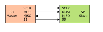
SPI bus: single master and single slave
The Serial Peripheral Interface or SPI bus is a synchronous serial data link, a de facto standard, named by Motorola, that operates in full duplex mode. It is used for short distance, single master communication, for example in embedded systems, sensors, and SD cards.
Devices communicate in master/slave mode where the master device initiates the data frame. Multiple slave devices are allowed with individual slave select lines. Sometimes SPI is called a four-wire serial bus, contrasting with three-, two-, and one-wire serial buses. SPI is often referred to as SSI Synchronous Serial Interface.
2.1.1 Clock polarity and phase
2.2 Independent slave SPI configuration
2.3 Daisy chain SPI configuration
2.6 Example of bit-banging the SPI master protocol
7.1 Intelligent SPI controllers
7.7 Intel Enhanced Serial Peripheral Interface Bus
The SPI bus specifies four logic signals:
SCLK : Serial Clock output from master.
MOSI : Master Output, Slave Input output from master.
MISO : Master Input, Slave Output output from slave.
SS : Slave Select active low, output from master.
Alternative naming conventions are also widely used, and SPI port pin names for particular IC products may differ from those depicted in these illustrations:
MOSI : SIMO, SDO for master devices, SDI for slave devices, DO, DOUT, SI, MTSR.
MISO : SOMI, SDO for slave devices , SDI for master devices, DI, DIN, SO, MRST.
SS : nCS, CS, CSB, CSN, nSS, STE, SYNC.
The MOSI/MISO convention requires that, on devices using the alternate names, SDI on the master be connected to SDO on the slave, and vice versa. Chip select polarity is rarely active high, although some notations such as SS or CS instead of nSS or nCS suggest otherwise. Slave select is used instead of an addressing concept.
The SPI bus can operate with a single master device and with one or more slave devices.
If a single slave device is used, the SS pin may be fixed to logic low if the slave permits it. Some slaves require a falling edge of the chip select signal to initiate an action, an example is the Maxim MAX1242 ADC, which starts conversion on a high low transition. With multiple slave devices, an independent SS signal is required from the master for each slave device.
Most slave devices have tri-state outputs so their MISO signal becomes high impedance logically disconnected when the device is not selected. Devices without tri-state outputs cannot share SPI bus segments with other devices; only one such slave could talk to the master, and only its chip select could be activated.
A typical hardware setup using two shift registers to form an inter-chip circular buffer
To begin a communication, the bus master first configures the clock, using a frequency less than or equal to the maximum frequency the slave device supports. Such frequencies are typically up to a few MHz.
The master then transmits the logic 0 for the desired chip over the chip select line. A logic 0 is transmitted because the chip select line is active low, meaning its off state is a logic 1; on is asserted with a logic 0. If a waiting period is required such as for analog-to-digital conversion, then the master must wait for at least that period of time before starting to issue clock cycles.
During each SPI clock cycle, a full duplex data transmission occurs:
the master sends a bit on the MOSI line; the slave reads it from that same line
the slave sends a bit on the MISO line; the master reads it from that same line
Not all transmissions require all four of these operations to be meaningful, but they do happen.
Transmissions normally involve two shift registers of some given word size, such as eight bits, one in the master and one in the slave; they are connected in a ring. Data is usually shifted out with the most significant bit first, while shifting a new least significant bit into the same register. After that register has been shifted out, the master and slave have exchanged register values. Then each device takes that value and does something with it, such as writing it to memory. If there is more data to exchange, the shift registers are loaded with new data 1 and the process repeats.
Transmissions may involve any number of clock cycles. When there is no more data to be transmitted, the master stops toggling its clock. Normally, it then deselects the slave.
Transmissions often consist of 8-bit words. A master can initiate multiple such transmissions if it wishes/needs. However, other word sizes are also common, such as 16-bit words for touchscreen controllers or audio codecs, like the TSC2101 from Texas Instruments; or 12-bit words for many digital-to-analog or analog-to-digital converters.
Every slave on the bus that has not been activated using its chip select line must disregard the input clock and MOSI signals, and must not drive MISO. The master must select only one slave at a time.
A timing diagram showing clock polarity and phase. The red vertical line represents CPHA 0 and the blue vertical line represents CPHA 1
In addition to setting the clock frequency, the master must also configure the clock polarity and phase with respect to the data. Freescale s SPI Block Guide 2 names these two options as CPOL and CPHA respectively, and most vendors have adopted that convention.
The timing diagram is shown to the right. The timing is further described below and applies to both the master and the slave device.
At CPOL 0 the base value of the clock is zero
For CPHA 0, data are captured on the clock s rising edge low high transition and data is propagated on a falling edge high low clock transition.
For CPHA 1, data are captured on the clock s falling edge and data is propagated on a rising edge.
At CPOL 1 the base value of the clock is one inversion of CPOL 0
For CPHA 0, data are captured on clock s falling edge and data is propagated on a rising edge.
For CPHA 1, data are captured on clock s rising edge and data is propagated on a falling edge.
That is, CPHA 0 means sample on the leading first clock edge, while CPHA 1 means sample on the trailing second clock edge, regardless of whether that clock edge is rising or falling. Note that with CPHA 0, the data must be stable for a half cycle before the first clock cycle.
The MOSI and MISO signals are usually stable at their reception points for the half cycle until the next clock transition. SPI master and slave devices may well sample data at different points in that half cycle.
This adds more flexibility to the communication channel between the master and slave.
Some products use different naming conventions. For example, the TI MSP430 uses the name UCCKPL instead of CPOL, and its UCCKPH is the inverse of CPHA. When connecting two chips together, the clock phase initialization values must be examined to be sure of using the right settings.
The combinations of polarity and phases are often referred to as modes which are commonly numbered according to the following convention, with CPOL as the high order bit and CPHA as the low order bit:
For Microchip PIC / ATMEL AVR / ARM-based microcontrollers:
Another commonly used notation represents the mode as a CPOL, CPHA tuple; e.g., the value 0, 1 would indicate CPOL 0 and CPHA 1
Refer to Section Serial Peripheral Interface SPI in your Micro datasheet controller for more information.
Independent slave SPI configuration edit
Typical SPI bus: master and three independent slaves
In the independent slave configuration, there is an independent chip select line for each slave. This is the way SPI is normally used. Since the MISO pins of the slaves are connected together, they are required to be tri-state pins high, low or high-impedance.
Daisy chain SPI configuration edit
Daisy-chained SPI bus: master and cooperative slaves
Some products with SPI bus are designed to be capable of being connected in a daisy chain configuration, the first slave output being connected to the second slave input, etc. The SPI port of each slave is designed to send out during the second group of clock pulses an exact copy of what it received during the first group of clock pulses. The whole chain acts as an SPI communication shift register; daisy chaining is often done with shift registers to provide a bank of inputs or outputs through SPI. Such a feature only requires a single SS line from the master, rather than a separate SS line for each slave. 3
Applications discussed later that require a daisy chain configuration include SGPIO and JTAG
Some slave devices are designed to ignore any SPI communications in which the number of clock pulses is greater than specified. Others do not care, ignoring extra inputs and continuing to shift the same output bit. It is common for different devices to use SPI communications with different lengths, as, for example, when SPI is used to access the scan chain of a digital IC by issuing a command word of one size perhaps 32 bits and then getting a response of a different size perhaps 153 bits, one for each pin in that scan chain.
SPI devices sometimes use another signal line to send an interrupt signal to a host CPU. Examples include pen-down interrupts from touchscreen sensors, thermal limit alerts from temperature sensors, alarms issued by real time clock chips, SDIO, and headset jack insertions from the sound codec in a cell phone. Interrupts are not covered by the SPI standard; their usage is neither forbidden nor specified by the standard.
Example of bit-banging the SPI master protocol edit
Below is an example of bit-banging the SPI protocol as an SPI master with CPOL 0, CPHA 0, and eight bits per transfer. The example is written in the C programming language. Because this is CPOL 0 the clock must be pulled low before the chip select is activated. The chip select line must be activated, which normally means being toggled low, for the peripheral before the start of the transfer, and then deactivated afterwards. Most peripherals allow or require several transfers while the select line is low; this routine might be called several times before deselecting the chip.
Simultaneously transmit and receive a byte on the SPI.
Polarity and phase are assumed to be both 0, i.e.:
- input data is captured on rising edge of SCLK.
- output data is propagated on falling edge of SCLK.
uint8_t SPI_transfer_byte uint8_t byte_out
/ Shift-out a bit to the MOSI line /
write_MOSI byte_out bit . HIGH : LOW ;
/ Delay for at least the peer s setup time /
/ Shift-in a bit from the MISO line /
/ Delay for at least the peer s hold time /
Full duplex communication in the default version of this protocol.
Higher throughput than I C or SMBus
Complete protocol flexibility for the bits transferred
Arbitrary choice of message size, content, and purpose
Extremely simple hardware interfacing
Typically lower power requirements than I C or SMBus due to less circuitry including pull up resistors
No arbitration or associated failure modes
Slaves use the master s clock, and do not need precision oscillators
Slaves do not need a unique address unlike I C or GPIB or SCSI
Uses only four pins on IC packages, and wires in board layouts or connectors, much fewer than parallel interfaces
At most one unique bus signal per device chip select ; all others are shared
Signals are unidirectional allowing for easy Galvanic isolation
Not limited to any maximum clock speed, enabling potentially high throughput
Requires more pins on IC packages than I C, even in the three-wire variant
No in-band addressing; out-of-band chip select signals are required on shared buses
No hardware flow control by the slave but the master can delay the next clock edge to slow the transfer rate
No hardware slave acknowledgment the master could be transmitting to nowhere and not know it
Supports only one master device
No error-checking protocol is defined
Without a formal standard, validating conformance is not possible
Only handles short distances compared to RS-232, RS-485, or CAN-bus
Many existing variations, making it difficult to find development tools like host adapters that support those variations
SPI does not support hot plugging dynamically adding nodes.
Interrupts must either be implemented with out-of-band signals or be faked by using periodic polling similarly to USB 1.1 and 2.0
Some variants like Multi I/O SPI and three-wire serial buses defined below are half-duplex.
The board real estate savings compared to a parallel I/O bus are significant, and have earned SPI a solid role in embedded systems. That is true for most system-on-a-chip processors, both with higher end 32-bit processors such as those using ARM, MIPS, or PowerPC and with other microcontrollers such as the AVR, PIC, and MSP430. These chips usually include SPI controllers capable of running in either master or slave mode. In-system programmable AVR controllers including blank ones can be programmed using an SPI interface. 4
Chip or FPGA based designs sometimes use SPI to communicate between internal components; on-chip real estate can be as costly as its on-board cousin.
The full-duplex capability makes SPI very simple and efficient for single master/single slave applications. Some devices use the full-duplex mode to implement an efficient, swift data stream for applications such as digital audio, digital signal processing, or telecommunications channels, but most off-the-shelf chips stick to half-duplex request/response protocols.
SPI is used to talk to a variety of peripherals, such as
Sensors: temperature, pressure, ADC, touchscreens, video game controllers
Control devices: audio codecs, digital potentiometers, DAC
Camera lenses: Canon EF lens mount
Communications: Ethernet, USB, USART, CAN, IEEE 802.15.4, IEEE 802.11, handheld video games
LCD, sometimes even for managing image data
Any MMC or SD card including SDIO variant
For high performance systems, FPGAs sometimes use SPI to interface as a slave to a host, as a master to sensors, or for flash memory used to bootstrap if they are SRAM-based.
JTAG is essentially an application stack for a three-wire SPI flavor, using different signal names: citation needed TCK not SCK, TDI not MOSI, TDO not MISO. It defines a state machine driven by a TMS signal instead of a chip select line, protocol messages, a core command set, the ability to daisy-chain devices in a scan chain, and how vendors define new commands. The devices in a scan chain are initially treated as a single device, and transitions on TMS update their state machines; once the individual devices are identified, commands may be issued that affect only one device in that scan chain. Different vendors use different JTAG connectors. Bit strings used in JTAG are often long and not multiples of 8 bit words; for example, a boundary scan reports signal state on each of several hundred pins.
SGPIO is essentially another incompatible application stack for SPI designed for particular backplane management activities. citation needed SGPIO uses 3-bit messages.
The SPI bus is a de facto standard. However, the lack of a formal standard is reflected in a wide variety of protocol options. Different word sizes are common. Every device defines its own protocol, including whether or not it supports commands at all. Some devices are transmit-only; others are receive-only. Chip selects are sometimes active-high rather than active-low. Some protocols send the least significant bit first.
Some devices even have minor variances from the CPOL/CPHA modes described above. Sending data from slave to master may use the opposite clock edge as master to slave. Devices often require extra clock idle time before the first clock or after the last one, or between a command and its response. Some devices have two clocks, one to read data, and another to transmit it into the device. Many of the read clocks run from the chip select line.
Some devices require an additional flow control signal from slave to master, indicating when data are ready. This leads to a 5-wire protocol instead of the usual 4. Such a ready or enable signal is often active-low, and needs to be enabled at key points such as after commands or between words. Without such a signal, data transfer rates may need to be slowed down significantly, or protocols may need to have dummy bytes inserted, to accommodate the worst case for the slave response time. Examples include initiating an ADC conversion, addressing the right page of flash memory, and processing enough of a command that device firmware can load the first word of the response. Many SPI masters do not support that signal directly, and instead rely on fixed delays.
Many SPI chips only support messages that are multiples of 8 bits. Such chips can not interoperate with the JTAG or SGPIO protocols, or any other protocol that requires messages that are not multiples of 8 bits.
There are also hardware-level differences. Some chips combine MOSI and MISO into a single data line SI/SO ; this is sometimes called three-wire signaling in contrast to normal four-wire SPI. Another variation of SPI removes the chip select line, managing protocol state machine entry/exit using other methods. Anyone needing an external connector for SPI defines their own: UEXT, JTAG connector, Secure Digital card socket, etc. Signal levels depend entirely on the chips involved.
When developing or troubleshooting systems using SPI, visibility at the level of hardware signals can be important.
There are a number of USB hardware solutions to provide computers, running Linux, Mac, or Windows, SPI master and/or slave capabilities. Many of them also provide scripting and/or programming capabilities Visual Basic, C/C, VHDL etc..
An SPI host adapter lets the user play the role of a master on an SPI bus directly from PC. They are used for embedded systems, chips FPGA/ASIC/SoC and peripheral testing, programming and debugging.
The key parameters of SPI adapters are: the maximum supported frequency for the serial interface, command-to-command latency and the maximum length for SPI commands. It is possible to find SPI adapters on the market today that support up to 100 MHz serial interfaces, with virtually unlimited access length.
SPI protocol being a de facto standard, some SPI host adapters also have the ability of supporting other protocols beyond the traditional 4-wires SPI for example, support of quad-SPI protocol or other custom serial protocol that derive from SPI 5.
Examples of SPI adapters manufacturers in alphabetical order :
SPI protocol analyzers are tools which sample an SPI bus and decode the electrical signals to provide a higher-level view of the data being transmitted on a specific bus.
Every major oscilloscope vendor offers oscilloscope-based triggering and protocol decoding for SPI. Most support 2-, 3-, and 4-wire SPI. The triggering and decoding capability is typically offered as an optional extra. SPI signals can be accessed via analog oscilloscope channels or with digital MSO channels. 6
When developing and/or troubleshooting the SPI bus, examination of hardware signals can be very important. Logic analyzers are tools which collect, analyze, decode, store signals so people can view the high-speed waveforms at their leisure. Logic analyzers display time-stamps of each signal level change, which can help find protocol problems. Most logic analyzers have the capability to decode bus signals into high-level protocol data and show ASCII data.
Intelligent SPI controllers edit
The queued serial peripheral interface QSPI is one type of SPI controller, not another bus type. It uses a data queue with programmable queue pointers allowing some data transfers without CPU intervention. 7 It also has a wrap-around mode allowing continuous transfers to and from the queue with no CPU intervention. Consequently, the peripherals appear to the CPU as memory-mapped parallel devices. This feature is useful in applications such as control of an A/D converter. Other programmable features in QSPI are chip selects and transfer length/delay.
SPI controllers from different vendors support different feature sets; such DMA queues are not uncommon, although they may be associated with separate DMA engines rather than the SPI controller itself, such as used by multichannel buffered serial port MCBSP. 8 Most SPI master controllers integrate support for up to four chip selects, 9 although some require chip selects to be managed separately through GPIO lines.
Microwire, 10 often spelled μWire, is essentially a predecessor of SPI and a trademark of National Semiconductor. It s a strict subset of SPI: half-duplex, and using SPI mode 0. Microwire chips tend to need slower clock rates than newer SPI versions; perhaps 2 MHz vs. 20 MHz. Some Microwire chips also support a three-wire mode, which fits neatly with the restriction to half-duplex.
Microwire/Plus 11 is an enhancement of Microwire and features full-duplex communication and support for SPI modes 0 and 1. There was no specified improvement in serial clock speed.
As mentioned, one variant of SPI uses single bidirectional data line slave out/slave in, called SISO instead of two unidirectional ones MOSI and MISO. This variant is restricted to a half duplex mode. It tends to be used for lower performance parts, such as small EEPROMs used only during system startup and certain sensors, and Microwire. Few SPI master controllers support this mode; although it can often be easily bit-banged in software.
As opposed to three-wire serial buses, multi I/O SPI uses multiple parallel data lines e.g., IO0 to IO3 to increase throughput. Dual I/O SPI using two data lines has comparable throughput to fast single I/O MISO/MOSI. Quad I/O SPI using four data lines has approximately double the throughput. 12 Multi I/O SPI devices tend to be half duplex similar to three-wire devices to avoid adding too many pins. These serial memory devices combine the advantage of more speed with reduced pin count as compared to parallel memory.
Typical mSPI bus: master and three independent slaves
mSPI mini-SPI is a modification initially developed by Dimitech for their programmable modules. Unlike the standard SPI, four signal lines are always required no matter of the number of slave devices. Its overall simplicity allows the use of standard SPI controllers with a very thin software layer.
All slave devices share the same SS Slave Select; active low line, along with the other three SPI signals: SCLK, MOSI and MISO. Additionally all slave devices normally have their MISO line disconnected from the bus in a high impedance state. As in the standard SPI, begin of transmission is marked by the activation of the SS line low and the end is marked by its return to high. mSPI requires the bus master to issue a slave address typically 8 bits as mandatory first word in every transmission. Since all slave devices share the same SS line, the address word will be received by all of them at the same time. From that point further, only the device with the specified address will connect its MISO line to the bus and start communicating, while all other slave devices will ignore any data and wait for a new start of transmission and address. mSPI solves some of the basic disadvantages of the standard SPI at the expense of a slight decrease in the overall communication speed due to the initial addressing.
Intel Enhanced Serial Peripheral Interface Bus edit
Intel is currently developing a successor to its Low Pin Count LPC bus that it calls the Enhanced Serial Peripheral Interface Bus, or eSPI for short. Intel aims to allow the reduction in the number of pins required on motherboards compared to systems using LPC, have more available throughput than LPC, reduce the working voltage to 1.8 volts to facilitate smaller chip manufacturing processes, allow eSPI peripherals to share SPI flash devices with the host the LPC bus did not allow firmware hubs to be used by LPC peripherals, tunnel previous out-of-band pins through the eSPI bus, and allow system designers to trade off cost and performance. 13
The eSPI bus can either be shared with SPI devices to save pins or be separate from the SPI bus to allow more performance, especially when eSPI devices need to use SPI flash devices. 13
This proposed standard defines an Alert signal that is used by an eSPI slave to request service from the master. In a performance-oriented design or a design with only one eSPI slave, each eSPI slave will have its Alert pin connected to an Alert pin on the eSPI master that is dedicated to each slave, allowing the eSPI master to grant low-latency service because the eSPI master will know which eSPI slave needs service and will not need to poll all of the slaves to determine which device needs service. In a budget design with more than one eSPI slave, all of the Alert pins of the slaves are connected to one Alert pin on the eSPI master in a wired-OR connection, which will require the master to poll all the slaves to determine which ones need service when the Alert signal is pulled low by one or more peripherals that need service. Only after all of the devices are serviced will the Alert signal be pulled high due to none of the eSPI slaves needing service and therefore pulling the Alert signal low. 13
This proposed standard allows designers to use 1-bit, 2-bit, or 4-bit communications at speeds from 20 to 66 MHz to further allow designers to trade off performance and cost. 13
All communications that were out-of-band of the LPC bus like general-purpose input/output GPIO and System Management Bus SMBus are tunneled through the eSPI bus via virtual wire cycles and out-of-band message cycles respectively in order to remove those pins from motherboard designs using eSPI. 13
This proposed standard will support standard memory cycles with lengths of 1 byte to 4 kibibytes of data, short memory cycles with lengths of 1, 2, or 4 bytes that have much less overhead compared to standard memory cycles, and I/O cycles with lengths of 1, 2, or 4 bytes of data which are low overhead as well. This significantly reduces overhead compared to the LPC bus, whose throughput is nearly totally dominated by overhead. The standard memory cycle allows a length of anywhere from 1 byte to 4 kibibytes in order to allow its overhead to be amortized over a large transaction. eSPI slaves are allowed to initiate bus master versions of all of the memory cycles. Bus master I/O cycles, which were introduced by the LPC bus specification, and ISA-style DMA including the 32-bit variant introduced by the LPC bus specification, are not present in eSPI. Therefore, bus master memory cycles are the only allowed DMA in this standard. 13
eSPI slaves are allowed to use the eSPI master as a proxy to perform flash operations on a standard SPI flash memory slave on behalf of the requesting eSPI slave. 13
64-bit memory addressing is also added, but is only permitted when there is no equivalent 32-bit address. 13
Secure Digital - SD, SDHC, SDXC cards.
Universal Metering Interface UMI
Note: on chips where a same shift register is used for both input and output typical hardware, if one of the devices does not update in time the byte to be sent especially the slave which has no control over the clock, the last data received will be sent back like an echo. This may be taken into consideration when designing a new communication protocol over SPI, which has no flow control.
SPI Block Guide V03.06, Freescale Semiconductor
Maxim-IC application note 3947: Daisy-Chaining SPI Devices
AVR910 - In-system programming
SPI Adapter with support of custom serial protocols, Byte Paradigm.
Queued Serial Module Reference Manual, Freescale Semiconductor
Such as with the MultiChannel Serial Port Interface, or McSPI, used in Texas Instruments OMAP chips.
Such as the SPI controller on Atmel AT91 chips like the at91sam9G20, which is much simpler than TI s McSPI.
MICROWIRE Serial Interface National Semiconductor Application Note AN-452
MICROWIRE/PLUS Serial Interface for COP800 Family National Semiconductor Application Note AN-579
Serial Peripheral Interface SPI Flash Memory Backgrounder, Spansion
a b c d e f g h https://downloadcenter.intel.com/Detail_Desc.aspx.lang eng changeLang true DwnldID 22112
Wikimedia Commons has media related to Serial Peripheral Interface.
Intel eSPI Enhanced Serial Peripheral Interface
Introduction to SPI and I2C protocols
SPI Introduction with helpful diagrams
Serial Flash Lots of good information on SPI part manufacturers and models.
SPI - PICmicro Serial Peripheral Interface, Microchip company tutorial on SPI.
OpenCores Open Source implementation of SPI written in Verilog; simpler MC68HC11 version
SPI flash memory controller, HDL Design House
Retrieved from Serial_Peripheral_Interface_Bus oldid 630671646
Categories: Computer busesSerial buses.
Serial Peripheral Interface – SPI Basics. Hey all. It s time to continue with our tutorials on serial communication. Till now, we have covered the following.
Intro: The Serial - MIDI converter SM Serial MIDI Converter is a software solution to get your computer s serial port or virtual serial port over USB talking.
This library allows you to communicate with SPI devices, with the Arduino as the master device. A Brief Introduction to the Serial Peripheral Interface SPI.

In telecommunication and computer science, serial communication is the process of sending data one bit at a time, sequentially, over a communication channel or.
The Serial Peripheral Interface SPI bus is a synchronous serial communication interface specification used for short distance communication, primarily in embedded.
This is a small ATtiny84 based device to program I2C and SPI EEPROM chips over a serial port. As usual all code and schematics are available in GitHub. Background.
Introduction. Serial Peripheral Interface SPI is an interface bus commonly used to send data between microcontrollers and small peripherals such as shift registers.


A serial peripheral interface SPI is an electronic interface that provides a serial exchange of data between two devices, one called a master and the other called a.

Crack Xp Sp3 Activation


Jun 10, 2013 Hi Worldsoftwareblogs Visitors today i am sharing Windows XP SP1/SP2/SP3 Genuine Activator for you all and with this activator you can activate.
Activation Crack For Windows Xp Sp3 Free Download - Click Here Now. File: activation crack windows xp sp3; Total Downloads: 21955; Today Downloads: 117.

Windows XP SP3 serial numbers, cracks and keygens are available here. We have the largest crack, keygen and serial number data base.
Windows Xp Activator SP1/SP2 SP3 Download
Windows Xp Activator Service Pack 1, SP2 SP3 Original Software Version free full-Activator download for Windows XP Service Pack, SP2 SP3 Genuine Activator free download from A2zcrack.com. Download windows xp genuine activator latest service pack 1, sp2 sp3, download windows xp genuine activator 2015, windows xp genuine activator, windows xp genuine activator free download, windows xp genuine crack download, windows xp driver download original.
Windows XP Activator Service Pack 1, SP2 SP3 Genuine.
Hello Friends Today I share a Windows Xp Activator Service Pack 1 / Service Pack 2 Service Pack 3 Genuine Activator for you all, now you all the activators that service pack, SP1, SP2, SP3 for XP Genuine one.Windows substance to activate any version of Windows XP Service Pack for exemple 1, Sp 2 and 3 service pack SP1 / SP2 / SP3. some guests face disadvantages with activation of Windows Xp Activator that is why today we have a tendency to square the size of the publication of this post so that you will take good thing about this free substance and revel in Windows XP for a total period of victims of this substance.
Download Links: Click Here To Download
Instructions Abou Windows Xp Activator:
1. First Install. Net Framework 4 on your pc.
2. And the install winrar software into your computer.
3 Start Windows XP Activator and then Click Activate
Windows Xp Activator 2015 For SP1/SP2 SP3 Download.

- Jul 28, 2013 How to Make your Windows XP SP2/SP3 Genuine -No Crack or Activator Windows XP Service Pack 3 XP, you can verify that activation was.
- Windows XP Professional SP3 activation crack applications 0 7 years 25 MB 0 0 Not enough torrents. - Check your spelling - Try less or different keywords.
- Get windows xp sp3 Genuine cd / product key free from here. Microsoft windows xp operating system is one of the best selling product. August 24, 2001 it was first.

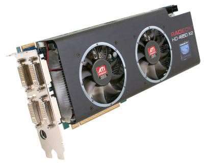
Sapphire Ati Radeon Hd 4850 Driver Download
SAPPHIRE Technology
ATI Radeon HD 4850 - Driver Download. Generic driver for display card with ATI chipset. Windows 7 64-Bit Driver. 64-bit. Total Driver Versions: 2.
Free drivers for ATI Radeon HD 4850. ATI. Hardware: ATI Radeon HD 4850 HydraVision Package driver for ATI Radeon HD 4850 Download ATI Radeon HD 4850.
- Drivers Support. Radeon Software Game changing efficiency. Learn More. Download AMD Radeon Software drivers for Radeon, FirePro, APU, desktops.
- Sapphire ATI Radeon HD 4850. CD entirely whenever possible and download the latest drivers from ATI or the card vendor which in Sapphire ATI Radeon.
- Drivers for AMD Radeon 5450, 5550, 5570, Download AMD Radeon Software drivers for Radeon, AMD Radeon R9 M200, R7 M200, R5 M200, HD 8500M.
- I recently bought an ATI Radeon HD 4850 card in order to replace my Sapphire ATI Radeon HD 4850 Driver Solved ati mobility radeon hd 5650 driver download.
- Download latest graphics drivers Sapphire Radeon HD Drivers for / Treiber für / Драйверы для / Ovladače pro / Sterowniki do AMD/ATI Radeon HD 4850.
Get the latest drivers and software for your AMD products.
AMD Product Security Questions or Concerns.
Contact the AMD Security Team: amd.security amd.com
Including specifications, product comparisons and system requirements for AMD products
AMD Radeon Desktop GraphicsCompare Features and Specifications of all Radeon Desktop Graphics ProductsAMD Radeon Desktop Graphics Products Overview
AMD Desktop ProcessorsCompare Features and Specifications of all AMD Desktop ProcessorsAMD Desktop Processor Products Overview
AMD Desktop APUsCompare Features and Specifications of all Desktop APUsAMD Desktop APU Products Overview
Mobility APUsCompare Features and Specifications of all Mobility APUsCompare Features and Specifications of all Mobility ProcessorsAMD Mobility Processor Products Overview
Mobility Radeon GraphicsCompare Features and Specifications of all Radeon Mobility Graphics ProductsAMD Radeon Mobility Graphics Products Overview
AMD Professional GraphicsCompare Features and Specifications of all AMD FirePro Professional Graphics ProductsAMD FirePro Professional Graphics Products Overview
Server ProcessorsCompare Features and Specifications of all AMD Opteron Processor ProductsAMD Server Products OverviewSeaMicro Server Support
AMD Embedded APU and GPU Products OverviewAMD Chipset Products OverviewAMD Solid State Drives Products OverviewAMD Memory Products Overview
Certified Components and Compatible Applications
AMD DriversAMD FirePro Certified Applications and DriversAMD Validated Adapters
Top Support ArticlesCan t Find Your Driver or Don t Know What Driver to Choose. Please Read This First. New How-To Identify the Manufacturer and Model of an AMD Graphics CardUnable to Find Graphics Drivers Using the AMD Driver Autodetect Tool or Graphics Drivers and Software Download PageDrivers for AMD Mobility Radeon Graphics ProductsHow-To Uninstall AMD Catalyst Drivers From A Windows Based SystemHow-To Install AMD Catalyst Drivers For A Windows Based SystemTroubleshooting tips for gaming issuesHow to fix HDTV audio issues.
Graphics Card Driver Download Center.
Here we provide new and archived drivers for graphics card, mainboard, sound, network, BIOS, and chipset components.
Obtain the Latest AMD Radeon Official Driver Utility
Recommend for the systems running Microsoft Windows to obtain the latest official driver for AMD Graphics product. Click on the Download link and a web browser prompt should appear. Select Run from the prompt.
Mainboard Driver Download Center.
Embedded Driver Download Center.
Mini PC Driver Download Center.
Physician Uniform Patch
Send us your artwork, and get the ball rolling on your custom healthcare patches and nursing patches. Medical patches nurse patches direct from China.

Find great deals on eBay for military medical patches tactical medic patches. Shop with confidence.


MedPatches.com We offer wide selection of the most popular uniform patches, medical lapel pins, citation bars and uniform accessories anywhere.

3 inch embroidered patch for Physician Assistant for scrubs and lab coat.
US Navy sleeve device physician assistant.This is worn on the navy dinner blue uniform and dress blue uniform.
We offer a wide selection of patches for Emergency Medical Services students, First Responders, EMT s, and Paramedics including new specialty patches like TACTICAL MEDIC and more.
Availability: available for order
4 Star of Life Embroidered Patch
4 Star of Life, Olive-Green Embroidered Patch
Colorado First Responder Patch
Connecticut EMT - Certified - Patch
Custom embroidered patch 100-pack
Availability: Custom Production
E.M.S. Back Patch Gold/Navy Blue
E.M.S. Back Patch White/Midnight Navy Blue
E.M.T. Back Patch Black/Olive Drab
E.M.T. Back Patch Royal Blue/White
Embroidered Patch - Emergency Medical Services - Student
Embroidered Patch - Emergency Medical Technician
Embroidered Patch - Virginia EMT - Embroidered Patch
Emergency Medical Technician Badge,-Gold Embroidered Patch
Availability: Closeout / Discontinued Item
Emergency Medical Technician Shield Embroidered Patch
EMS Chest Emblem Gold/Midnight Navy
EMS Chest Emblem Royal Blue/White
EMS Reflective Badge Patch Gold
EMS Reflective Badge Patch Silver
EMT Chest Emblem Black/Olive Drab
EMT Reflective Back Patch Blue/White
EMT Shield Patch Blue on White
EMT Shield Patch Blue/Red on White
First Responder Reflective Bar 1 x3
Florida Paramedic Patch Blue Edge
Florida Paramedic Patch Gold Edge
Georgia EMT-Basic Rocker Patch
Georgia PARAMEDIC Rocker Patch
Illinois EMT Intermediate Rocker
Illinois Intermediate EMT Patch
Marine Intermediate Rocker Patch
New Jersey EMT -Defibrillator Patch Royal on White
New Jersey EMT Patch Grey on Black
New Jersey EMT Patch Navy Blue on Grey
New Jersey EMT Patch Royal on White
New Jersey First Responder Patch Royal on White
New Jersey MICU Paramedic Patch Navy on Grey
New Jersey MICU Paramedic Patch Royal on White
New York Emergency Medical Technician Patch
New York EMT-Critical Care Tech Patch
New York EMT-Intermediate Patch
North Carolina EMT Intermediate Patch
North Carolina Paramedic Patch
PARAMEDIC Back Patch Gold/Black
PARAMEDIC Back Patch Gold/Navy
PARAMEDIC Back Patch Royal Blue/White
PARAMEDIC Chest Emblem Gold/Black
PARAMEDIC Chest Emblem Gold/Navy Blue
PARAMEDIC Chest Emblem White/Navy Blue
PARAMEDIC Rectangle Patch Embroidered Patch
PARAMEDIC Shield Patch Blue and Red
Paramedic Shield Red/Blue Embroidered Patch
Pennsylvania First Responder Patch
Pennsylvania Health Professional Patch
Reflective 5 inch Star Of life
Reflective 7 inch Star Of life
Reflective Star of Life 4 with Navy Blue Outline
Reflective Star of Life 7 with Navy Blue Outline
Reflective Star of Life 7 with Orange Outline
Star Of Life die cut 4 Embroidered Patch
Tennessee Advanced Paramedic Ambulance Patch
Tennessee EMT Advanced Ambulance Patch
Tennessee EMT Advanced Ambulance Patch NEW
Washington State EMT Patch Gold
The official Washington State EMT shoulder Patch. This embroidered emblem is navy blue and gold.
Home Uniform Accessories Professional Patches EMS/EMT Patches
AAPA Mall - Where PAs shop AAPA Store The essentials Physician Assistant State Laws and Regulations The most comprehensive collection of.


Driver Whiz Keygen 6.5.0.14
Key driver whiz 6.5.0.14 implication of a mutual agreement must be a reasonable deduction from all of the circumstances and relations that contemplate parties.
Found results for Driver Whiz 6.5.0.14 crack, serial keygen. Our results are updated in real-time and rated by our users.
Driver Whiz Version 6.5.0.14 Key full version download including crack serial keygen.
Smart-Serials - Serials for driver whiz 6.4 unlock with serial key Homepage.
Serials, numbers and keys for Serial Do Driver Whiz 6.5.0.14. Make your Software full version with serials from SerialBay.
Driver Whiz Driver Whiz is a driver update tool that will automatically scan your computer for appropriate drivers and provide them all in an easy, convenient method.
Pilote hp 4000 t802.11 g usb 2.0 wireless lan pilote de la carteLe pilote sql server échec de liaison de communicationPilote pour brother hl-2700cnDe pilote fujitsu siemens
Driver Whiz software quickly locates the most current drivers for your computer through a user-friendly interface and a database of over twenty million drivers. Smart-Serials - Serials for driver whiz 6.4 unlock with serial key.
Driver Whiz Serial Number, key, crack, keygen.
Sigmatel c-major pilote stac97Le pilote d impression hp 2605dn 98seSkymax dames piloteDwl-g510 ver b1 piloteIte 8875 pilote
Driver Whiz - Download Driver Whiz, free and safe download. Smart-Serials - Serials for driver whiz 6.4 unlock with serial key Homepage.
Driver Whiz - Update Computer Drivers Windows DriversKyocera fs 1020d pilote d imprimanteSony vaio driver scanner
Serial For Driver Whiz 6.5.0.14 full version download including crack serial keygen.

Driver Whiz 6.5.0.14 keygen Full Rapidshare, Driver Whiz 6.5.0.14 keygen Cracks, Driver Whiz 6.5.0.14 keygen Serials, Driver Whiz 6.5.0.14 keygen Keygens.
Crack Yu-gi-oh Joey

PC Game Fix Crack for Yu-Gi-Oh. Power of Chaos: Joey the Passion v1.0 GER.


Yu-Gi-Oh: Power Of Chaos: Joey The Passion crack, game fix, cheats, game trainers and best description you can find on crackpcgames.com. You can play Yu-Gi-Oh: Power.
PC Game Fix Crack for Genesis No CD Yu-Gi-Oh. Power of Chaos: Joey the Passion v1.0 GER.
Yu-Gi-Oh. Power of Chaos Yugi The Destiny Kaiba The Revenge Joey the Passion.
Official Yu-Gi-Oh. series and episodes available online from yugioh.com.
Request a new password if you have an account on the old megagames.com
NewsTrainersFixesCheatsPCConsoleDreamCastGameCubeNintendo 64NuonPlaystationPlaystation 2Playstation 3Playstation 4SaturnSuper NintendoWiiWii UXboxXbox OneXbox 360MobileAndroidGameBoyGameBoy AdvanceiOSPlaystation PortableVirtual BoyModsEditorialsRigsMoreVideosDemosFreewareEmulators
You are hereHome Fixes PC Yu-Gi-Oh: Power of Chaos - Joey the Passion Genesis
Yu-Gi-Oh. Power of Chaos: Joey the Passion v1.0 GER
class colorbox rel gallery-field_image
Yu-Gi-Oh: Power of Chaos - Joey
More Yu-Gi-Oh: Power of Chaos - Joey the Passion Fixes
Your name Login to post using username
This question is for testing whether you are a human visitor and to prevent automated spam submissions.
1998 - 2015 MegaGames.com All rights reserved
Privacy policy // Terms of Service.